
Silicon carbide epitaxy equipment belongs to the field of semiconductor equipment and occupies a key upstream link in the third-generation semiconductor industry chain. Our silicon carbide epitaxy equipment adopts independent innovative structural design, and is compatible with 6-inch and 4-inch epitaxial wafer growth. It is the first completely independent and innovative silicon carbide epitaxy equipment in China with excellent process indicators, low cost of consumables and low maintenance frequency. .
PRODUCTS & TECHNOLOGY

(1) MOCVD equipment: MOCVD equipment for controllable and batch preparation of new two-dimensional materials
(2) CVD equipment: According to the specific needs put forward by customers, tailor-made CVD equipment is mainly used to synthesize two-dimensional materials such as graphene, TMD, and nanomaterials required for scientific research.
(3) Other semiconductor equipment technologies mastered by the company's R&D team can be used in ALD, PECVD, MOCVD and etching equipment of various materials.
For the preparation of transition metal sulfide TMDs such as tungsten sulfide, indium selenide, boron nitride, etc.
China's open roll-to-roll chemical vapor deposition equipment can continuously prepare large-area graphene thin film materials on a large scale for 24 hours, improving preparation efficiency and reducing production costs.
Integration*: Copper foil cleaning and polishing -> pretreatment -> graphene growth -> graphene transfer -> graphene device preparation, etc. are integrated into one production line, reducing intermediate links
Clean and polish the purchased coil copper foil to provide raw copper foil that can grow high-quality graphene; transfer the produced graphene from copper foil to PET to provide transfer graphene that meets customer needs.
The CVD graphene prepared by our company is a high-quality, single-layer and continuous thin-film material grown on the copper foil medium under the condition of lower than the lowest explosion limit of hydrogen and methane. CVD graphene materials have been industrialized in batches, including transparent conductive films, transparent heating films, photoelectric sensors, transparent generating films, and flexible heating wearable devices.
ADVANTAGE MATERIAL


ABOUT US
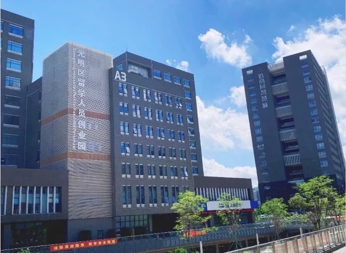
Shenzhen Naso Tech Co., Ltd. was established in October 2018 and is located in the Overseas Students Pioneer Park in Guangming District, Shenzhen. With the vision of becoming a global leader in advanced material manufacturing equipment and the mission of improving China's advanced material manufacturing capacity, the company is committed to the R & D, production, sales, application and promotion of advanced material manufacturing equipment such as the third generation semiconductor and graphene.
The company was rated as a "national high-tech enterprise" with high growth in 2020. In addition, the company's third-generation semiconductor silicon carbide high temperature chemical vapor deposition epitaxial equipment technology was listed in the list of leading technologies of "Kechuang China"; Won the "best compound semiconductor equipment technology development award" of Shenzhen integrated circuit industry association.
Learn moreNEWS CENTER

Website
Copyright © 2021 Shenzhen Nashe Intelligent Equipment Co., Ltd. All rights reserved. 粤ICP备20057176号
Powered by 300.cn | SEO